Interfaces between 2D and 3D Materials: Graphene on SiO2 (alpha-quartz).
1. Introduction
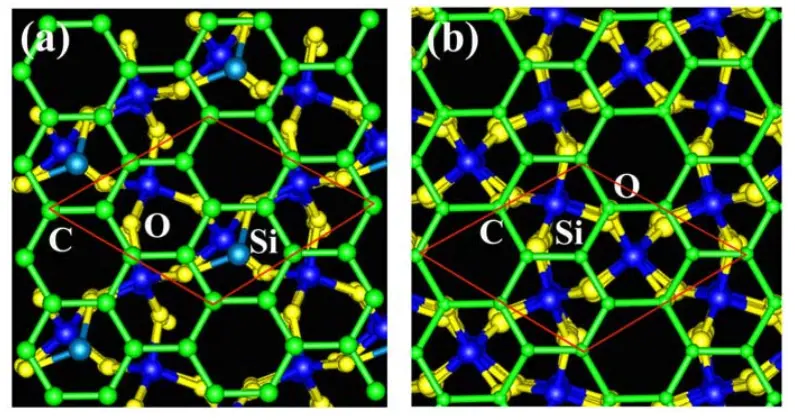
This tutorial demonstrates the process of creating interfaces between 2D and 3D materials, specifically graphene and silicon dioxide (SiO2), based on the work presented in the following manuscript, where the electronic properties of graphene on SiO2 are studied.
Manuscript
Yong-Ju Kang, Joongoo Kang, and K. J. Chang "Electronic structure of graphene and doping effect on SiO2" Physical Review B 78, 115404 (2008) DOI: 10.1103/PhysRevB.78.115404 12
We use the Materials Designer to create interfaces between graphene and silicon dioxide with oxygen termination, as shown in the manuscript.
We will focus on replicating the metastable geometry of Kang et al. Sec. III: graphene 2.58 Å above the O-terminated surface, shifted from the C-over-O registry of Fig. 1(b).
2. Load and Preview Materials
Navigate to Materials Designer and import graphene and silicon dioxide materials from the Standata.
Then use the JupyterLite environment to create the target structures.
3. Create Interface Between Graphene and Silicon Dioxide
2.1 Launch JupyterLite Session
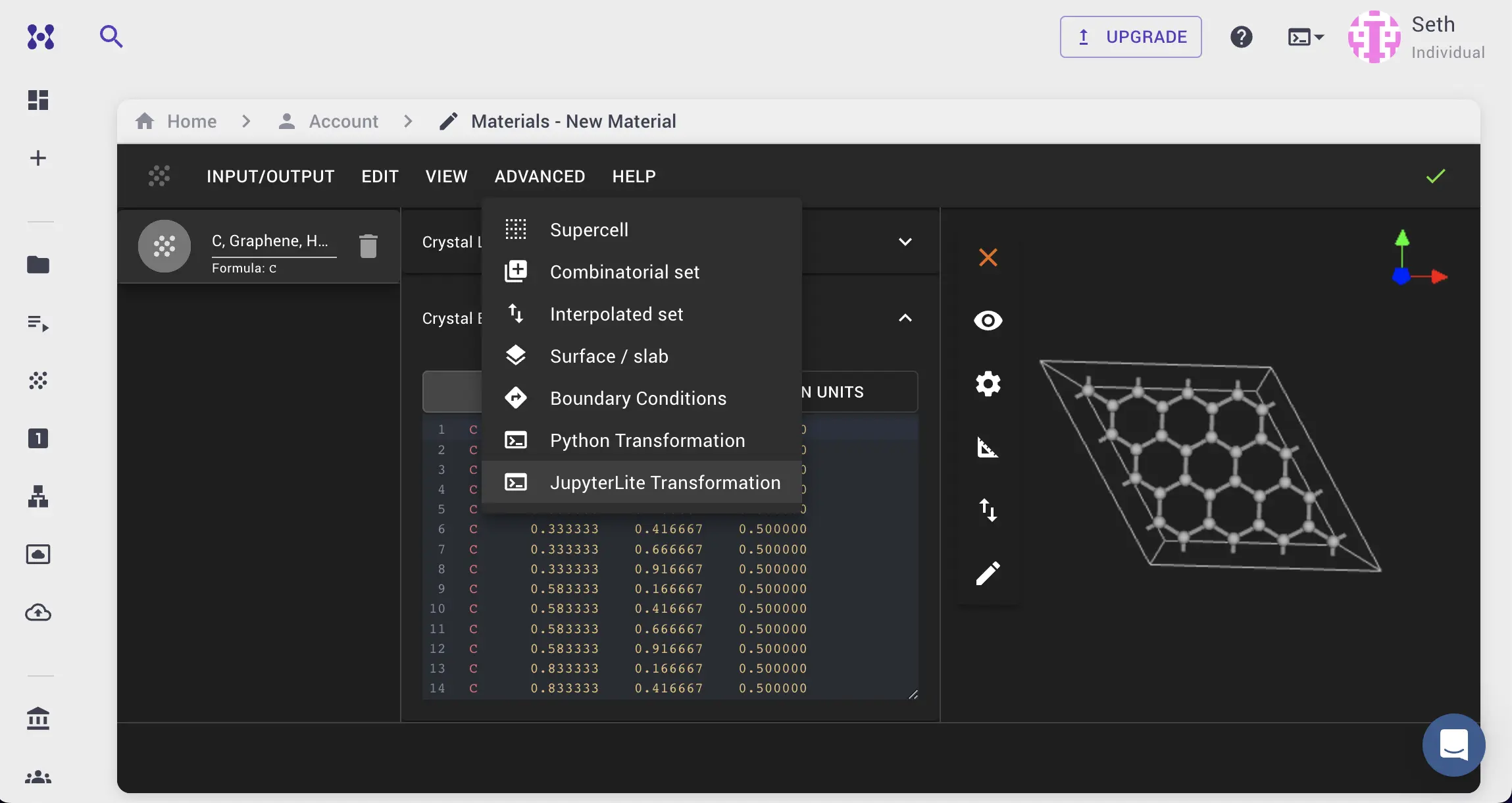
Select the "Advanced > JupyterLite Transformation" menu item to launch the JupyterLite environment.
2.2 Open and Modify the Notebook
Select the input materials with the first being the substrate (SiO₂) and the second being the film (graphene).
Open the create_interface_with_min_strain_zsl.ipynb notebook and modify the parameters as follows:
- Miller indices:
(0, 0, 1)for both materials - Thickness:
1layer for graphene,5layers for SiO₂ (5 conventional cells: 15 Si planes; the manuscript has 14 bilayers) - Interface distance:
2.58Å (as stated in the manuscript) - Interface vacuum:
17.5Å (gives about 20 Å above graphene, as specified in the manuscript)
Let's set MAX_AREA=150 Ų to allow for a larger search area for the superlattice search algorithm.
TERMINATION_PAIR_INDICES will be set to [1] to get the O-terminated interface as shown in the manuscript.
Adjust the "1.1. Set up slab parameters" cell as shown:
1 2 3 4 5 6 7 8 9 10 11 12 13 14 15 16 17 18 19 20 21 22 23 24 25 26 27 28 29 30 31 32 33 34 35 36 | |
The specific-example notebook interface_2d_3d_graphene_silicon_dioxide.ipynb continues after the ZSL step with two more cells, which the generic notebook does not have. The ZSL match leaves the registry of graphene on the quartz surface undefined. The notebook shifts the film in-plane by REGISTRY_SHIFT to the registry of the manuscript's metastable geometry (Sec. III), where one surface O sits near a C atom and the other near a hexagon centre, and prints each surface O's in-plane distance to the nearest C. Its parameter, set in the notebook's parameter cell, and cell 3.5:
1 | |
1 2 3 4 5 6 7 8 9 10 11 12 13 14 15 16 | |
Cell 3.6 puts the cell in the 120° hexagonal setting and centers the slab along z, so that no atom sits at z = 0, where a relaxation would wrap it to the top of the cell:
1 2 3 4 5 6 7 8 | |
2.3 Run the Notebook
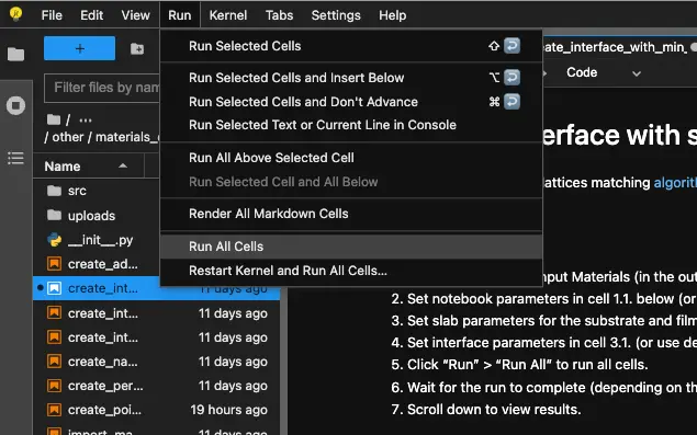
Run the notebook to generate the interface structure between graphene and silicon dioxide with oxygen termination.
3.4. View Results
The generation might take some time. After that, the user can pass the material to the Materials Designer for further analysis.
4. Pass the Material to Materials Designer
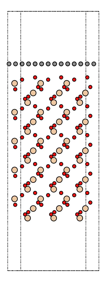
After generating the interface structure, pass the material to the Materials Designer for further analysis.
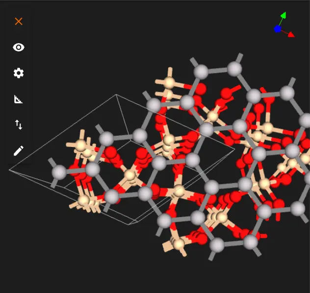
The interface between graphene and silicon dioxide with oxygen termination is shown below.
5. Interactive JupyterLite Notebook
The interactive JupyterLite notebook for creating interfaces between graphene and silicon dioxide is embedded below. To run the notebook, click on the "Run All" button.
6. References
-
Yong-Ju Kang, Joongoo Kang, and K. J. Chang. Electronic structure of graphene and doping effect on sio2. Physical Review B, 78:115404, 2008. URL: https://link.aps.org/doi/10.1103/PhysRevB.78.115404. ↩
-
Arjun Dahal and Matthias Batzill. Graphene–nickel interfaces: a review. Nanoscale, 6:2548–2562, 2014. URL: https://doi.org/10.1039/C3NR05279F. ↩